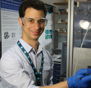
An international team of scientists from the University of Leuven in Belgium, the National University of Singapore and CSIRO have masterminded a new method to grow designer crystals that could ultimately lead to a new breed of faster, more powerful electronic devices.

Image credit: www.csiro.au
These crystals, also known as “metal organic frameworks” or MOFs, are the world’s most porous materials, and if applied to microelectronic devices, could significantly boost their processing power.
Up until now, these crystals could only be grown and applied using a liquid solvent, which has proven to corrode and damage components, making them unsuitable for electronics applications.
CSIRO researcher Mark Styles said the new method abandons the use of a liquid solvent and uses vapour instead. According to him, the vapour method overcomes this barrier and has the potential to disrupt the microelectronics industry.
“Just like your smart phone doesn’t like being dropped in water, electronic devices don’t like the liquid solvent that’s used to grow MOF crystals. It can corrode and damage the delicate circuitry,” Dr Styles said in a news release.
“On the atomic scale, MOF crystals look like bird cages that can be tailor-made to be different shapes and sizes. They have an extremely large surface area, meaning they can be up to 80 per cent empty inside. The net result is a structure where almost every atom is exposed to empty space: one gram of MOF crystals has a surface area of over 5000 square metres – that’s the size of a football field.”
He said the team can use this vast space to trap other molecules, which can change the properties of a material.
“In the case of electronics, this means we can fit a lot more transistors on a microchip, making it faster and far more powerful,” Mr Styles added.
He said the team drew on specialist X-ray analysis techniques from CSIRO and the Australian Synchrotron to learn how the vapour process works, and how it can be used to grow the MOF crystals.
According to Mr Styles, the applications for MOFs are virtually limitless.
“Another potential use for this technology would be in portable chemical sensing devices that could be used in hazardous environments such as chemical processing plants and underground mines,” he said.
To read the Nature Materials paper, please go to: Chemical vapour deposition of zeolitic imidazolate framework thin films.


