

Scientists from CSIRO and Germany’s Fraunhofer Institute for Mechanics of Materials have developed a diamond-coated yarn which could reduce costs in the solar and semiconductor industries.
Copyright: Fraunhofer IWM
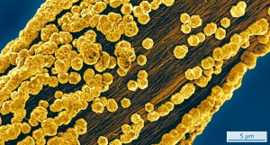
Fraunhofer Institute physicist Manuel Mee has developed a way to coat ultra-thin, extremely stable nanothreads with diamond to make them much stronger than steel wires, allowing them to be manufactured more finely.
“The new saw wires held out the promise of being far superior to traditional steel wires,” Mr. Mee said, quoted in a media release from Austrade.
“Because of their high tensile strength, they can be manufactured much thinner than steel wires – and that means significantly less kerf loss.”
Kerf loss is basically saw dust, but the expensive kind. According to CSIRO, electronics manufacturers also have to deal with saw dust, although on a microscopic scale.
“When making electronics products, manufacturers have to cut through high-tech materials – like semiconductors and silicon wafers – meaning lots of tiny particles end up going to waste,” writes Crystal Ladiges on the CSIRO blog.
“As these materials are very expensive, this wastage turns out to be a much bigger problem than it is for your average tradie.”
To overcome the wastage issue, CSIRO and Fraunhofer Institute developed the diamond-coated saw wire that is set to effect dramatic reductions in kerf loss.
According to Fraunhofer Institute, the coated nanotubes have various possible applications such as being a component of highly sensitive sensors and thermoelectric generators.
The new material however is extremely difficult to synthesize as diamonds only grow under extreme conditions. The tricky process also means the compound used to encourage diamonds to grow on nanotubes damages the nanotubes.
Dr. Mee however found a solution to this problem.
“During our first experiments, fused silica from the reaction chamber accidentally came into contact with the coating plasma. It settled on the substrate and protected it against the aggressive hydrogen,” he said.
“We had to study the silicon oxide layer, which was deposited in an undefined manner, and find a method of controlling the deposition and optimizing the process.”
Subsequent tests done in CSIRO’s lab revealed that the nanotubes actually survived under their protective layer.
According to Austrade both organizations have filed a joint patent application for the process and related products. They are also conducting tests to bring the development to market as quickly as possible.
“To be able to show our partners in industry the potential the technology holds, we have to demonstrate how it can help solar companies save material when processing wafers,” Mr. Mee said.


