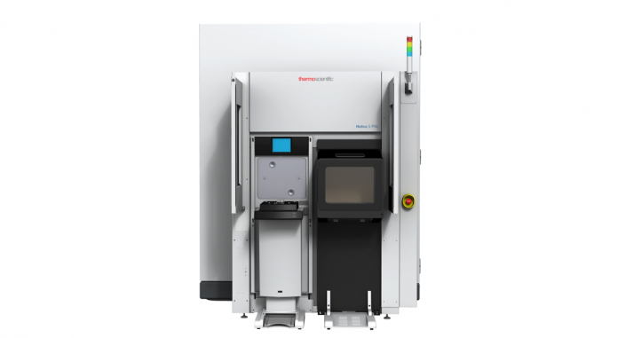
The Thermo Scientific Helios 5 PXL PFIB Wafer DualBeam is a fully automated system designed to decrease time-to-data for through-stack metrology from days to hours.
US-based scientific instrumentation provider Thermo Fisher Scientific unveiled today its latest scanning electron microscope (SEM), the Thermo Scientific Helios 5 PXL PFIB Wafer DualBeam.
The Helios 5 PXL, which offers high-resolution and high-contrast imaging, leverages focused ion beams to reduce time-to-data from days to hours for inline through-stack metrology and verification of high-aspect ratio structures.
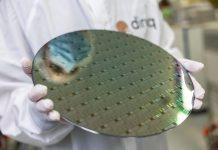
The system can also provide sample deprocessing, diagonal milling and cross sectioning of advanced 3D semiconductor devices, such as 3D NAND and advanced memory.
Vice president and general manager of semiconductor at Thermo Fisher Glyn Davies explained: “As layer counts increase, the manufacturing process for current and future high-aspect-ratio structures is becoming increasingly complex.
“With this breakthrough system, already being used by a global leader in semiconductor manufacturing, high-volume fabrication customers will be able to measure thousands of metrology points at multiple positions in the 3D stack for high aspect ratio and buried structures.”
Thermo Fisher’s latest entry is compatible with semiconductor factory automation, facilitating operator-free operations and supporting high-throughput requirements of fab metrology and process monitoring.
Other benefits of the Helios 5 PLX include:
- Nanometer-scale SEM imaging;
- High-volume, high-speed milling and cross sectioning;
- Optimized planar deprocessing for high sensitivity materials and surface quality preservation;
- Deprocessing of advanced metallization layers through proprietary chemistries;
- Precise, site-specific preparation of large-area lamellae with the optional Thermo Scientific EasyLift Nanomanipulator; and
- Full coverage of 300 wafer handling.
For more information about the Helios 5 PXL, visit https://ter.li/Helios5PXL.


